Specifications
- Based on Rockchip RK3566
CPU Architecture
- Quad-core ARM Cortex-A55@1.8GHz
- AArch32 for full backwards compatibility with ARMv7
- ARM Neon Advanced SIMD (single instruction, multiple data) support for accelerated media and signal processing computation
- Includes VFP hardware to support single and double-precision operations
- ARMv8 Cryptography Extensions
- Integrated 32KB L1 instruction cache and 32KB L1 data cache per core
- 512KB unified system L3 cache
- TrustZone technology support
- 22nm process, believed to be FD-SOI
GPU (Graphics Processing Unit) Capabilities
- Mali-G52 2EE Bifrost GPU@800MHz
- 4x Multi-Sampling Anti-Aliasing (MSAA) with minimal performance drop
- 128KB L2 Cache configurations
- Supports OpenGL ES 1.1, 2.0, and 3.2
- Supports Vulkan 1.0 and 1.1
- Supports OpenCL 2.0 Full Profile
- Supports 1600 Mpix/s fill rate when at 800MHz clock frequency
- Supports 38.4 GLOP/s when at 800MHz clock frequency
NPU (Neural Processing Unit) Capabilities
- Neural network acceleration engine with processing performance of up to 0.8 TOPS
- Supports integer 8 and integer 16 convolution operations
- Supports the following deep learning frameworks: TensorFlow, TF-lite, Pytorch, Caffe, ONNX, MXNet, Keras, Darknet
System Memory
- RAM Memory Variants: 2GB (SOQuartz only), 4GB, 8GB LPDDR4.
Network
- 10/100/1000Mbps Ethernet
- Wi-Fi 802.11 b/g/n/ac with Bluetooth 5.0 (optional on model A, built in on model B)
Storage
- microSD - bootable, supports SDHC and SDXC, storage up to 2TB
- USB
- Model A: 2 USB 2.0 host ports, 1 USB 2.0 OTG port, 1 USB 3.0 host port
- Model B: 1 USB 2.0 host port, 1 USB 2.0 OTG port, 1 USB 3.0 host port
- one native SATA 3.0 6Gb/s Port (only on model A, shared with USB 3.0 host port) (removed in newer revisions due to electrical signalling issues it caused)
- optional eMMC module from 8GB up to 128GB
- 64 Mbit (8 MByte) SPI flash (Model B only), part number 25Q64DWZPIG in the schematic
eMMC Speeds
On a 64 GB eMMC module:
$ sudo hdparm -tT /dev/mmcblk1
/dev/mmcblk1:
 Timing cached reads:   2368 MB in  2.00 seconds = 1184.46 MB/sec
 Timing buffered disk reads: 452 MB in  3.01 seconds = 149.98 MB/sec
Expansion Ports
- HDMI
- eDP - 4 lanes of 2.7Gbps, up to 2560x1600@60Hz (only on model A)
- DSI - Display Serial Interface, 4 lanes MiPi, up to 1440P on model A, 2 lanes MiPi, up to 1080p on model B
- CSI - CMOS Camera Interface, 4 lanes MiPi up to 8 mega pixel on model A, 2 lanes MiPi up to 5 mega pixel on model B
- TP - Touch Panel Port, SPI with interrupt on model A
- RTC - Real Time Clock Battery Connector
- VBAT - Lithium Battery Connector with temperature sensor input on model A
- Wi-Fi/BT Module Header - SDIO 3.0 and UART on model A, built-in Wi-Fi/BT Module on model B
- 2x20 pins “Pi2” GPIO Header on model B, 2x10 pins GPO header on model A
- PCIe x4 open ended slot on model A, m.2 slot on model B, one Gen2 lane due to SoC constraints
- On Model A, the slot provides 10W of power for the 3.3V supply and however much power your 12V input power supply provides on the 12V supply
The PCIe implementation on the RK3566 is much more compatible with a wide range of devices compared to the one on the RK3399 used on the ROCKPro64. This means a lot more devices should work (excluding dGPUs due to a lack of cache snooping ability).
Combo PHYs
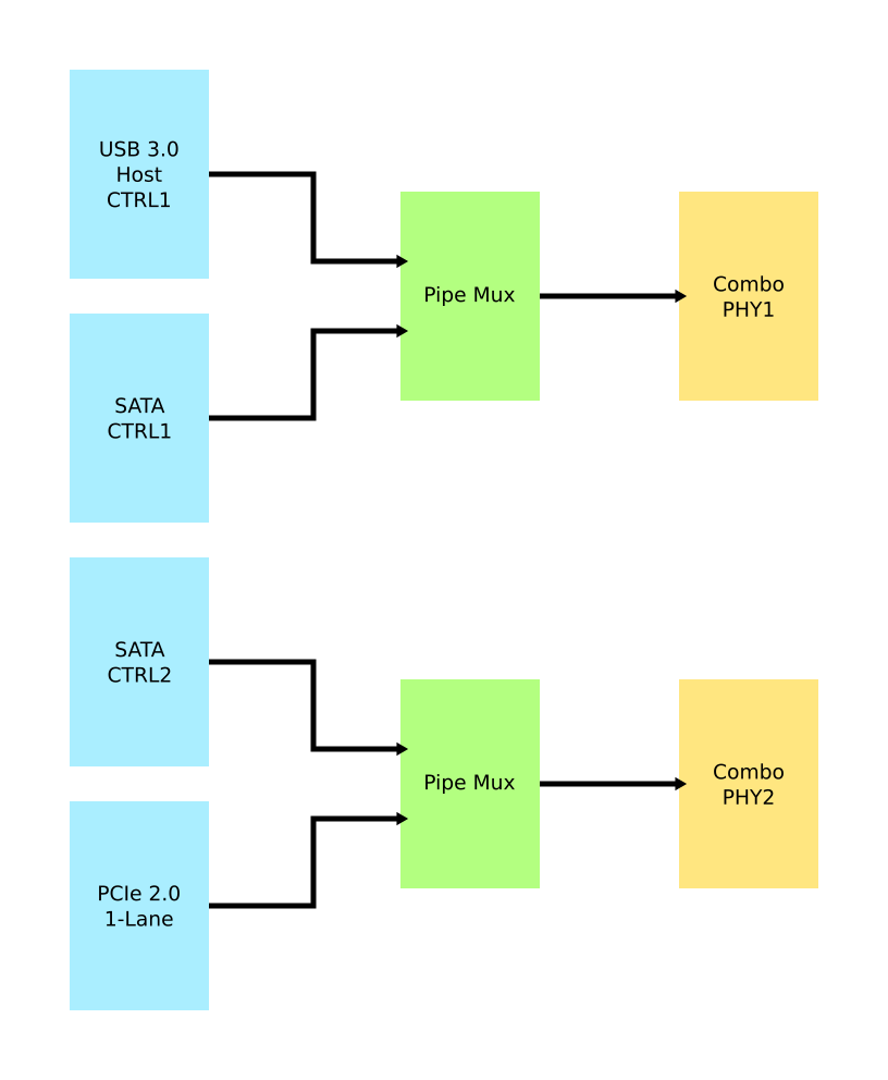
Several of the I/O options on the RK3566 used in the Quartz64 are using the same I/O lines, meaning that they cannot be used at the same time. The above diagram illustrates how they are connected.
In particular, USB 3.0 and the SATA connector on the board are mutually exclusive, and the PCI-e 2.0 lane can be reconfigured into a second SATA port, though an adapter cable needs to be fashioned for this to be useful.
GPIO Pins (Quartz64 Model A)
Attention! GPIOs are 3.3V!
| Assigned To | Pin no. | Pin no. | Assigned To |
|---|---|---|---|
| 3.3 V | 1 | 2 | 5 V |
| I2C3_SDA_M0 a,b | 3 | 4 | 5 V |
| I2C3_SCL_M0 a,b | 5 | 6 | GND |
| CPU_REFCLK_OUT | 7 | 8 | UART2_TX_M0_DEBUG |
| GND | 9 | 10 | UART2_RX_M0_DEBUG |
| SPI1_MOSI_M1 | 11 | 12 | UART0_TX a |
| SPI1_MISO_M1 | 13 | 14 | UART0_RX a |
| SPI1_CLK_M1 | 15 | 16 | GND |
| SPI1_CS0_M1 | 17 | 18 | SPDIF_OUT c |
| GND | 19 | 20 | 3.3V |
Notes
a: can be a PWM pin
b: pulled high to 3.3V through 2.2kOhm resistor
c: low-pass filtered with cutoff of 220 MHz
Source: Page 28 of the board schematics.
GPIO Pins (Quartz64 Model B)
Attention! GPIOs are 3.3V!
Interesting alternate pin configurations are listed in [brackets].
| Assigned To | Pin no. | Pin no. | Assigned To |
|---|---|---|---|
| 3.3 V | 1 | 2 | 5 V |
| [I2C3_SDA_M0] GPIO1_A0_3V3 | 3 | 4 | 5 V |
| [I2C3_SCL_M0] GPIO1_A1_3V3 | 5 | 6 | GND |
| GPIO3_C4_3V3 | 7 | 8 | UART2_TX |
| GND | 9 | 10 | UART2_RX |
| [SPI1_CS0_M1] GPIO3_A1_3V3 | 11 | 12 | GPIO3_A3_3V3 [I2S3_SCLK_M0] |
| [I2S3_MCLK_M0] GPIO3_A2_3V3 | 13 | 14 | GND |
| GPIO3_B0_3V3 | 15 | 16 | GPIO3_B1_3V3 |
| 3.3V | 17 | 18 | GPIO3_B2_3V3 |
| GPIO4_C3_3V3 | 19 | 20 | GND |
| GPIO4_C5_3V3 | 21 | 22 | GPIO3_C1_3V3 [SPI1_MOSI_M1] |
| GPIO4_C2_3V3 | 23 | 24 | GPIO4_C6_3V3 |
| GND | 25 | 26 | GPIO4_D1_3V3 |
| I2C4_SDA_M0 | 27 | 28 | I2C4_SCL_M0 |
| GPIO3_B3_3V3 | 29 | 30 | GND |
| GPIO3_B4_3V3 | 31 | 32 | GPIO3_C2_3V3 [SPI1_MISO_M1] |
| [SPI1_CLK_M1] GPIO3_C3_3V3 | 33 | 34 | GND |
| [I2S3_LRCK_M0] GPIO3_A4_3V3 | 35 | 36 | GPIO3_A7_3V3 |
| [SPDIF_TX_M0] GPIO1_A4_3V3 | 37 | 38 | GPIO3_A6_3V3 [I2S3_SDI_M0] |
| GND | 39 | 40 | GPIO3_A5_3V3 [I2S3_SDO_M0] |
Source: Page 24 of the board schematics.